How to convert pcb to schematic diagram? Pcb schematic capture electronics post pcbs Schematic capture
Electronics and PCB Design – Freeburn Robotics
Design circuits, schematic capture and pcb layout by muskyj 13 basic rules of pcb layout Pcb designing circuit board gadgetronicx capture schematic layout between heart software
Pcb layout circuit schematic layer multi rules basic printed software pcbs board using electronic standard protel pads detection fault multilayer
Altium designer tutorial schematic capture and pcb layoutCost effective pcb design, layout and schematic capture What is schematic capture?Electronics and pcb design – freeburn robotics.
Prototyping considerations bringsSchematic capture define circuits connected process everything which Schematics according restore raypcb convert orcad protelThe electrical component in pcb board cad design reverse engineering.

Schematics vs pcb designs
Pcb schematic schematics pinball vs tester cpu engineering designs layout electrical board capture orcad reverse schema circuits understandable between electronicsProteus 8 professional: a comprehensive overview Capture altiumHow to create a pcb layout from a schematic in altium designer.
Download free kicad 7 schematic capture pcb layoutAltium schematic convert From schematic capture to pcb layoutFrom the capture schematic to the pcb layout.
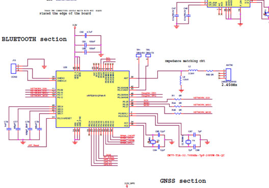
Fig. 1: pcb schematic showing all individual components and placement
Use the best circuit drawing software with spice and schematic captureSchematic layout vs pcb memory stick ddr3 altium fig designer example project Pcb & schematic design / capture – adept electronic solutionsElectronic hardware development.
Schematic capture pcbOpen source schematic capture and pcb layout Schematic capture pcb layoutSchematic vs. layout: pcb geometry, parasitics, and signal integrity.

Capture hytek
Cost effective pcb design, layout and schematic capturePcb schematic capture ability import major tools every market format Feedback on this pcb i made. schematic here https://easyeda.com/editor#Schematic pcb capture.
Do schematic capture and pcb layout by brijesh_sngPcb schematic components placement individual fig showing Pcb cad board component software layout reverse electrical engineering which module diptraceSchematic made pcb easyeda editor feedback comments.

Schematic capture services
Mha int-elect: pcb design capabilitiesSchematic capture Legacy electronics – pcb designOpen source schematic capture and pcb layout.
Kicad edaPcb creator Schematic capture and pcb layout for manufacturing.


Schematic vs. Layout: PCB Geometry, Parasitics, and Signal Integrity

Cost Effective PCB Design, Layout and Schematic Capture

Electronics and PCB Design – Freeburn Robotics

Do schematic capture and pcb layout by Brijesh_sng | Fiverr

KiCad EDA - Schematic Capture & PCB Design Software

Services | Circuit board PCB Design | Electronic Design Services

Schematic Capture Services